- 您现在的位置:买卖IC网 > Sheet目录1998 > ICS844071AGLFT (IDT, Integrated Device Technology Inc)IC CLOCK GEN GIG ETH 8-TSSOP
ICS844071AG REVISION B OCTOBER 10, 2012
3
2012 Integrated Device Technology, Inc.
ICS844071 Data Sheet
FEMTOCLOCK CRYSTAL-TO-LVDS CLOCK GENERATOR
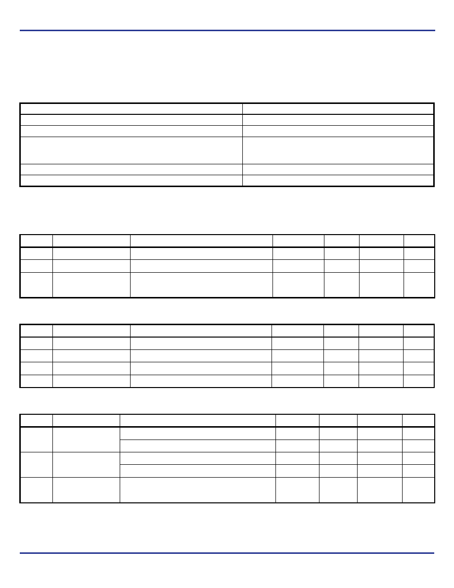
Absolute Maximum Ratings
NOTE: Stresses beyond those listed under Absolute Maximum Ratings may cause permanent damage to the device.
These ratings are stress specifications only. Functional operation of product at these conditions or any conditions beyond
those listed in the DC Characteristics or AC Characteristics is not implied. Exposure to absolute maximum rating conditions for
extended periods may affect product reliability.
DC Electrical Characteristics
Table 3A. Power Supply DC Characteristics, VDD = 3.3V ± 10%, TA = 0°C to 70°C
Table 3B. Power Supply DC Characteristics, VDD = 2.5V ± 5%, TA = 0°C to 70°C
Table 3C. LVCMOS/LVTTL DC Characteristics, VDD = 3.3V ± 10% or 2.5V ± 5%, TA = 0°C to 70°C
Item
Rating
Supply Voltage, VDD
4.6V
Inputs, VI
-0.5V to VDD + 0.5V
Outputs, IO
Continuous Current
Surge Current
10mA
15mA
Package Thermal Impedance,
θ
JA
101.7
°C/W (0 mps)
Storage Temperature, TSTG
-65
°C to 150°C
Symbol
Parameter
Test Conditions
Minimum
Typical
Maximum
Units
VDD
Core Supply Voltage
2.97
3.3
3.63
V
VDDA
Analog Supply Voltage
VDD – 0.12
3.3
3.63
V
IDD
Power Supply Current
135
mA
IDDA
Analog Supply Current
12
mA
Symbol
Parameter
Test Conditions
Minimum
Typical
Maximum
Units
VDD
Core Supply Voltage
2.375
2.5
2.625
V
VDDA
Analog Supply Voltage
VDD – 0.12
2.5
2.625
V
IDD
Power Supply Current
120
mA
IDDA
Analog Supply Current
12
mA
Symbol
Parameter
Test Conditions
Minimum
Typical
Maximum
Units
VIH
Input High Voltage
VDD = 3.3V
2
VDD + 0.3
V
VDD = 2.5V
1.7
VDD + 0.3
V
VIL
Input Low Voltage
VDD = 3.3V
-0.3
0.8
V
VDD = 2.5V
-0.3
0.7
V
IIH
Input High Current
VDD = VIN = 3.63V or 2.625V
5
A
IIL
Input Low Current
VDD = 3.63V or 2.625V, VIN = 0V
-150
A
发布紧急采购,3分钟左右您将得到回复。
相关PDF资料
ICS844201BG-45LF
IC CLK GENERATOR 25MHZ 8TSSOP
ICS844204BK-245LF
IC CLK SYNTHESIZER 4LVDS 32VFQFN
ICS844S42BKILF
IC SYNTHESIZER RF FREQ 56-VFQFPN
ICS86004BG-01LF
IC CLK BUFFER ZD 1:4 16-TSSOP
ICS8634BY-01LFT
IC BUFFER ZD 1-5 LVPECL 32-LQFP
ICS8701AY-01LF
IC CLK GEN POLARITY CTRL 48-LQFP
ICS8701CYLF
IC CLK GENERATOR /1 /2 48-LQFP
ICS870931ARI-01LF
IC CLK GENERATOR LVCMOS 20QSOP
相关代理商/技术参数
ICS844201BG-45LF
功能描述:IC CLK GENERATOR 25MHZ 8TSSOP RoHS:是 类别:集成电路 (IC) >> 时钟/计时 - 专用 系列:HiPerClockS™, FemtoClock™, PCI Express® (PCIe) 标准包装:1,500 系列:- 类型:时钟缓冲器/驱动器 PLL:是 主要目的:- 输入:- 输出:- 电路数:- 比率 - 输入:输出:- 差分 - 输入:输出:- 频率 - 最大:- 电源电压:3.3V 工作温度:0°C ~ 70°C 安装类型:表面贴装 封装/外壳:28-SSOP(0.209",5.30mm 宽) 供应商设备封装:28-SSOP 包装:带卷 (TR) 其它名称:93786AFT
ICS844201BG-45LFT
功能描述:IC CLK GENERATOR 25MHZ 8TSSOP RoHS:是 类别:集成电路 (IC) >> 时钟/计时 - 专用 系列:HiPerClockS™, FemtoClock™, PCI Express® (PCIe) 标准包装:1,500 系列:- 类型:时钟缓冲器/驱动器 PLL:是 主要目的:- 输入:- 输出:- 电路数:- 比率 - 输入:输出:- 差分 - 输入:输出:- 频率 - 最大:- 电源电压:3.3V 工作温度:0°C ~ 70°C 安装类型:表面贴装 封装/外壳:28-SSOP(0.209",5.30mm 宽) 供应商设备封装:28-SSOP 包装:带卷 (TR) 其它名称:93786AFT
ICS844201BGI-45LF
功能描述:IC CLK GENERATOR 25MHZ 8TSSOP RoHS:是 类别:集成电路 (IC) >> 时钟/计时 - 专用 系列:HiPerClockS™, FemtoClock™, PCI Express® (PCIe) 标准包装:1,500 系列:- 类型:时钟缓冲器/驱动器 PLL:是 主要目的:- 输入:- 输出:- 电路数:- 比率 - 输入:输出:- 差分 - 输入:输出:- 频率 - 最大:- 电源电压:3.3V 工作温度:0°C ~ 70°C 安装类型:表面贴装 封装/外壳:28-SSOP(0.209",5.30mm 宽) 供应商设备封装:28-SSOP 包装:带卷 (TR) 其它名称:93786AFT
ICS844201BGI-45LFT
功能描述:IC CLK GENERATOR 25MHZ 8TSSOP RoHS:是 类别:集成电路 (IC) >> 时钟/计时 - 专用 系列:HiPerClockS™, FemtoClock™, PCI Express® (PCIe) 标准包装:1,500 系列:- 类型:时钟缓冲器/驱动器 PLL:是 主要目的:- 输入:- 输出:- 电路数:- 比率 - 输入:输出:- 差分 - 输入:输出:- 频率 - 最大:- 电源电压:3.3V 工作温度:0°C ~ 70°C 安装类型:表面贴装 封装/外壳:28-SSOP(0.209",5.30mm 宽) 供应商设备封装:28-SSOP 包装:带卷 (TR) 其它名称:93786AFT
ICS844202AK-245LF
功能描述:IC CLOCK GEN SRL SCSI 32-VFQFPN RoHS:是 类别:集成电路 (IC) >> 时钟/计时 - 专用 系列:HiPerClockS™, PCI Express® (PCIe) 标准包装:28 系列:- 类型:时钟/频率发生器 PLL:是 主要目的:Intel CPU 服务器 输入:时钟 输出:LVCMOS 电路数:1 比率 - 输入:输出:3:22 差分 - 输入:输出:无/是 频率 - 最大:400MHz 电源电压:3.135 V ~ 3.465 V 工作温度:0°C ~ 85°C 安装类型:表面贴装 封装/外壳:64-TFSOP (0.240",6.10mm 宽) 供应商设备封装:64-TSSOP 包装:管件
ICS844202AK-245LFT
功能描述:IC CLOCK GEN SRL SCSI 32-VFQFPN RoHS:是 类别:集成电路 (IC) >> 时钟/计时 - 专用 系列:HiPerClockS™, PCI Express® (PCIe) 标准包装:28 系列:- 类型:时钟/频率发生器 PLL:是 主要目的:Intel CPU 服务器 输入:时钟 输出:LVCMOS 电路数:1 比率 - 输入:输出:3:22 差分 - 输入:输出:无/是 频率 - 最大:400MHz 电源电压:3.135 V ~ 3.465 V 工作温度:0°C ~ 85°C 安装类型:表面贴装 封装/外壳:64-TFSOP (0.240",6.10mm 宽) 供应商设备封装:64-TSSOP 包装:管件
ICS844202AKI-245LF
功能描述:IC CLOCK GEN SRL SCSI 32-VFQFPN RoHS:是 类别:集成电路 (IC) >> 时钟/计时 - 专用 系列:HiPerClockS™, PCI Express® (PCIe) 标准包装:1,500 系列:- 类型:时钟缓冲器/驱动器 PLL:是 主要目的:- 输入:- 输出:- 电路数:- 比率 - 输入:输出:- 差分 - 输入:输出:- 频率 - 最大:- 电源电压:3.3V 工作温度:0°C ~ 70°C 安装类型:表面贴装 封装/外壳:28-SSOP(0.209",5.30mm 宽) 供应商设备封装:28-SSOP 包装:带卷 (TR) 其它名称:93786AFT
ICS844202AKI-245LFT
功能描述:IC CLOCK GEN SRL SCSI 32-VFQFPN RoHS:是 类别:集成电路 (IC) >> 时钟/计时 - 专用 系列:HiPerClockS™, PCI Express® (PCIe) 标准包装:28 系列:- 类型:时钟/频率发生器 PLL:是 主要目的:Intel CPU 服务器 输入:时钟 输出:LVCMOS 电路数:1 比率 - 输入:输出:3:22 差分 - 输入:输出:无/是 频率 - 最大:400MHz 电源电压:3.135 V ~ 3.465 V 工作温度:0°C ~ 85°C 安装类型:表面贴装 封装/外壳:64-TFSOP (0.240",6.10mm 宽) 供应商设备封装:64-TSSOP 包装:管件